Calibration of the Linear Regime of Photodiode Detector
Huijie Miao
SUNY at Stony Brook
Optics Rotation Project 2
Advisor: Thomas Weinacht
ˇ¤ Introduction and
Motivation
ˇ¤ Photodiode Detector
ˇ¤ Experimental Setup and Results
ˇ¤ Acknowledgements
Introduction and Motivation
The following diagram(fig.1)
shows the construction of the photodiode which we used for the detector.
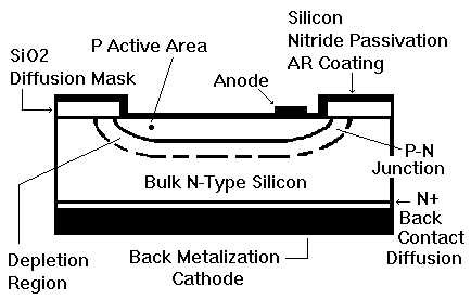
fig. 1
The silicon photodiode is
constructed from single crystal silicon wafers. It requires high
purity silicon. In fact, it is just a PN junction device. The ˇ°pˇ± layer is very
thin, which is formed by thermal diffusion or ion implantation of the
appropriate doping material (usually boron). The front contact is the anode and
the back contact is the cathode. The active area is covered by some
antireflection coating which is optimized for particular irradiation
wavelengths.
According to the characteristics of semi-conductor, we
know, at normal temperature, the thermal energy produces a
ˇ°depletion regionˇ± around the PN junction. The width of the depletion region
can be changed by applying a voltage across the photodiode. If a positive
voltage is in contact with the N type end of the diode while a negative voltage
is in contact with the P type end of the diode, which means we reverse bias the
diode, the depletion region will be enlarged. The majority carriers in P region
(holes) are attracted by the negative voltage, which draws them away from the
depletion region. And the majority carriers in N region (electrons) are drew
away from the depletion region by the positive voltage. The attractive forces
result an enlargement of the depletion region, consequently, the energy gap
between the two regions.
The reverse-biasing results in a large sensitivity for
detecting radiation. And the output voltage of the photodiode is extremely
linear with respect to the power applied to the photodiode junction. However, a
too high input power may cause the photodiode saturated. It means when the
input is higher the some certain value, the output voltage doesnˇŻt change
obviously with it.
Since the price of a photodiode
detector(phototransistor) is more then $100, and the price of a photodiode is
just around $20, we want to make the detector with the photodiode ourselves.
ThatˇŻs our main motivation for the project. Further, we calibrated the linear
regime of the detector. This project is pretty practicable and attractive.
Photodiode Detector
Fig.2 shows
the circuit which we followed to make the detector.
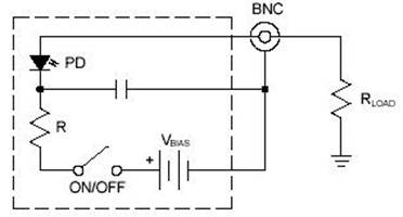
fig. 2
The photodiode we used is FDS010-Photodiode, SI. The rising time is £1ns (Measured with 50W load and 12V bias), the active area is 0.8mm2 (Æ1.0mm) and the spectral range is 200~1100nm.
Here are some
values we picked up for the circuit:
Capacitance:
0.1µF
Resistance: 1kW
VBIAS = 9V (reverse)
Fig.3
shows the detector which we made in our laboratory.
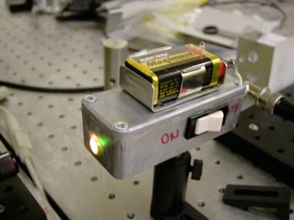
fig. 3
Experimental Setup and Results
Here is the experimental setup. The light source is Ti : Sapphire laser pulses, whose period is about 1 ps. An changeable aperture is used to control the input power. A fast lens is placed between the light source and the photodiode to make sure that all the light will be focused onto the detector. Thus the calibration will be independent on the size of the light spot. To avoid to burned the photodiode, a ND filter is used to lower the intensity of the input light. The filter we use is with ND=3, which mean it will lower the input power by 1000 times. Fig.4 and fig.5 show the setup in our lab.
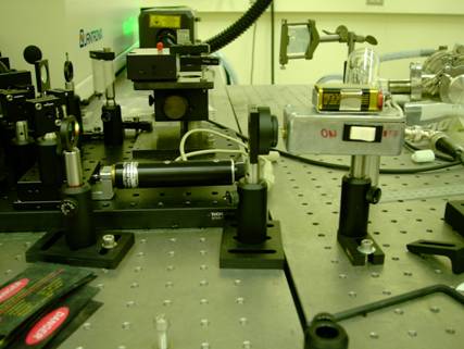
fig. 4
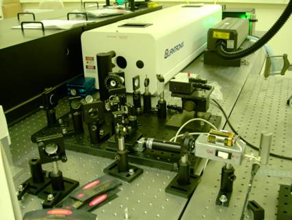
fig. 5
We measured 24 dots to calibrate the linear regime of the detector. Fig.6 gives the result of our calibration.
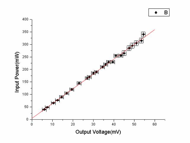
fig. 6
Y = A + B * X
Parameter
Value Error
-----------------------
A 4.03 0.61
B 5.93 0.04
R N
0.99949 24
The linear correlation coefficient R is 0.999, so the
linearity of the response is quite good. And we got the relation between the
input power and the output voltage. Thus we calibrated the linear regime for
the detector successfully. It works just like a power meter. We can use it to
tell the laser power easily. However, because the spectral response of the
photodiode (shown in fig.7), if we use it for other wavelength laser, we need
to calibrate it again. But for the Ti : Sapphire laser
in our lab, it is effective.
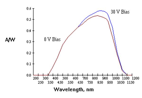
fig. 7
Acknowledgements
Professor Weinacht helped me a lot with my project. He helped me to pick up such an interesting and practicable topic, introduce me the most basic facilities in the lab, encouraged me to use them and gave me many useful advises. Under his guidance, I became familiar with the atmosphere in the lab. I am so grateful to his generous help. Also, I want to thank my lab matesˇŞPatrick and David. They always lend me a hand when I encountered problems.