Nano-electrode Multi-well High-gain Avalanche Rushing Photoconductor (NEW-HARP)
Background
Amorphous Selenium (a-Se), previously developed for photocopying machines, has become commercially used in x-ray photoconductors for Flat-Panel Detectors (FPDs). However, current FPDs are limited by degradation of low-dose imaging performance due to electronic noise. The energy required to generate an electron-hole pair in a-Se is extremely high and unreliable to constantly reproduce perfectly.
Technology
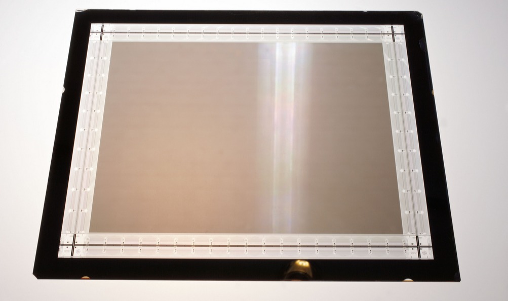
This technology is a Time of flight (TOF) detector including a scintillator, a common electrode, a pixel electrode, a multitude of insulating layers with a multitude of nano-pillars formed in a large group of insulating layers, and a nano-scale well structure between adjacent nano-pillars (where a-Se separates them). a-Se is used as the photoconductive material; this provides a radiation detector that solves the disadvantages of conventional detectors. The method of detection includes detecting the motion of holes throughout a region that includes a large amount of electrodes, insulating layers, and a substrate including nano-pillars. The a-Se is injected between adjacent nano-pillars when this technology is manufactured.
Advantages
Ultra-fast photo response - ultra-high time resolution
Application
Solid-state Imaging detectors of ionizing Radiation - Amorphous selenium Radiation detectors
Inventors
Wei Zhao, Professor, Radiology
Amirhossein Goldan, Assistant Professor, Radiology
John Rowlands, Professor,
Licensing Potential
Development partner,Commercial partner,Licensing
Licensing Status
Available for licensing.
Licensing Contact
Donna Tumminello, Assistant Director, Intellectual Property Partners, donna.tumminello@stonybrook.edu, 6316324163
Patent Status
Patented
Stage of Development
[US Patent 9,941,428](http://patft.uspto.gov/netacgi/nph-Parser?Sect1=PTO1&Sect2=HITOFF&d=PALL&p=1&u=%2Fnetahtml%2FPTO%2Fsrchnum.htm&r=1&f=G&l=50&s1=9941428.PN.&OS=PN/9941428&RS=PN/9941428)
Tech ID
8535